
Our Honorable Prime minister of India Shri. Narendra Modi ji Vision is “Fostering Next Generation Capabilities Among Chip Designers For Making India Self-Reliant In Electronics System Design” In order to achieve , Chips to Startup (C2S) Programme aims to train 85,000 number of Specialized Manpower over a period of 5 years in the area of VLSI and Embedded System Design and leapfrog in ESDM space by way of inculcating the culture of System-on-Chip (SoC)/ System Level Design at Bachelors, Masters and Research level and act as a catalyst for To establish the base of ASIC/IC design in the country by accommodating more academic institutions, Startups for design of IPs/ASICs/SOCs/Systems.
The main objectives of the C2S Program are:
• To protect Intellectual Property generated and to inculcate the culture of entrepreneurship among students and researchers by incubating Startups.
• To promote industry –led R&D translational research and strengthening industry academia collaboration.
• To develop the culture of developing reusable IP Cores, ASIC/SCO systems for societal /Strategic sectors
• To generate industry ready manpower in system/SOC Design area for creating vibrant fables chip design ecosystem in the country. Growth of Start-ups involved in fables design.
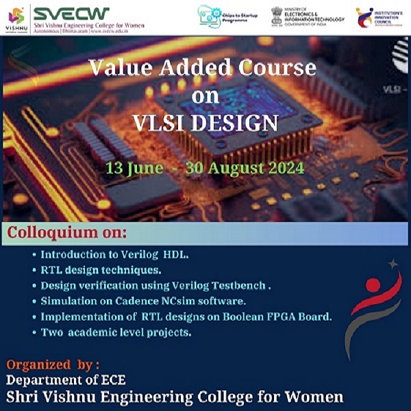
The Department of Electronics and Communication Engineering, Shri Vishnu Engineering College for Women is honored to receive a project titled “Memory Optimized Co-Processor for Enhanced Edge AI” under the Chips to Start up Program funded by Ministry of Electronics and Information Technology (MEITy).
Project Outlay
Name of Institute : Shri Vishnu Engineering College for Women (Autonomous), Bhimavaram,
Title of the project : Memory Optimized Co-Processing Unit for Enhanced edge AI
Total outlay of project : Rs. 64.5 Lakhs
Duration of project: 5 Years
Name of Chief Investigator (CI)/ Co-CI associated with the project
Dr. K. Padma Vasavi- Chief Investigator
Dr. MV Ganeswara Rao- Co Investigator
Dr. MV Subba Rao – Co Investigator
Mr. G. Challaram- Co Investigator
Resources Received under C2S Project:
- Centralized Electronic Design Automation (EDA) tools facility
- Modern FPGA Boards
- Instruction Enhancement Programmes (IEPs)
- Skilled Manpower Advanced Research and Training (SMART) facility
- Organizing Workshops/Symposiums/Conferences/Webinars
- Chip Design Infrastructure
- Creation of reusable IPs repository
- Protection of Intellectual Property (IPs) Core Generated
- India Chip Programme
EDA Tools and Boards Received under C2S Project
| S. No | Name of the EDA Tool | Product Description |
| 1 | AMD Xilinx VITIS | VITIS ,Vivado Tools, Vitis High Level Synthesis, Vitis Model Compressor, Matsim Addon |
| 2 | Cadence | Full custom IC design Bundle, Semi-custom IC Design Bundle SCL PDK for tapeout |
| 3 | Synopsys | Front end and Back-end Bundles, Full Custom Bundle, TCAD and 2D TCAD Bundles |
| 4 | Siemens | Tanner EDA, Calibre EDA, Questa EDA, Tessent EDA, Oasys, Nitro,Precision RTL synthesis, Catapult |
| 5 | Silvaco | TCAD (Semiconductor Process and Device Simulators), Analog Custom IC Design – EDA Tools, Standard Cell Library Development Tools, IPs |
| 6 | Ansys | HFSS, Totem, RedHawk, Power Artist EDA, RaptorX, Sea Scape |
| 7 | Keysight | Advanced Design System, Kliosoft Software, , Quantumpro, System Vue Software |
| 8 | FPGA Boards | PynqZ2, Urbana Boards, Boolean Boards, Xilinx Ultrascale Boards, Zynq, Kria Boards |
Broad Objectives of Project
- Design and develop a specialized co-processing unit tailored for edge AI applications with a focus on efficient memory management.
- To evaluate its performance by integrating the memory-optimized CPU with real-world edge AI applications
- To use a hybrid approach by prototyping the proposed design on FPGA first and implement the same using ASIC after fault detection and correction using FPGA
- To fabricate the proposed design to implement Memory Optimization in the processor.
Activities Done Under the Project
Outcomes


Patent
A patent is published based on the partial work done under the project with preliminary results